In the January I did the teardown of Amazon Echo Dot (3rd Gen). When recently, their 5th Generation of Amazon Echo Dot came, I was curious what changes they might have done to improve the performance of the device and what new features they have added and how 🙂

So what is new in the Amzon Echo Dot 5th Generation, it is basically provides better experience with much clear voice quality, deeper bass, better sound quality
Additionally a temperature sensor is also added to measure ambient temperature.
In this version Amazon has used their in-house developed Wi-Fi Connectivity equipment with Mesh technology (as a PCB module).
What is the difference from User point of view?
- Amazon Echo Dot 5 doesn’t have Aux Audio port, so you cannot connect it to any other device via audio port.
- Amazon Echo Dot 5 has a larger speaker measuring 1.73 inches with an improved audio quality.
- Amazon Echo Dot 5 has a new in-built temperature sensor.
- Amazon Echo Dot 5 and Echo Dot 4 are of same size (100 x 100 x 89mm).
Now, let us dive in and see how it is built.
Packaging is absolutely fantastic.
In the box, you will get the Amazon Echo Dot, User Manual and 12V at 1.25A 15W charger. And, the charger is also designed by Amazon only.
I purchased this from Amazon.in for around 4500 INR.


the power supply which comes with the Amazon Echo Dot 5th Gen is a 15W(12V, 1.25A) 230V AC Adapter with a DC Pin. It would have been in my opinion to provide a USB-C type connector for the Power.

Amazon Echo Dot from outside is not very different than its previous version.


To further open you need see the bottom side, rubber pad is there, once you remove that, you will get access to the screws which need to be opened to get inside.
Clearly mentioned Assembled in CHINA.


The 9 pads you see from the square hole is basically for programming and testing in the production.


Amazon Echo Dot 5th Gen MIC Array PCB
Once you remove the screws and open, you can see this:
In the left picture you see plastic diffuser ring which comes on the top of the LED, this helps spreading the light from the LEDs equally.
You can also see a RFID tag, that is mainly used in the manufacturing for tracking the devices or parts.
In the other 3 images what you see is the main controller board which has the main power supply, processor and LED ring, Wi-Fi Connectivity.


There is another PCB, which has MEM MIC, ambient light sensor and Button, this PCB is basically connected to the main PCB via Flexible cable.


Plastic structure which holds the four buttons and provides MIC access via PCB holes.

The MIC array PCB looks like this: It has 3 MICs (MK1, MK2, MK4), provision for 4th(MK3) one but not mounted. all 4 MIC connections are going to Texas Instruments IC TLV320ADC5140.
Three Microphones are used for beam forming to know the direction of the audio and also used for noise cancellation.


The TLV320ADC5140 is a Burr-Brown™ high performance, audio analog-to-digital converter (ADC)
that supports simultaneous sampling of up to four analog channels or eight digital channels for the pulse density modulation (PDM) microphone input.

There are several regulators on board like U3, VR1.


There are two more ICs – U6 and U1(45575 N211J UAA), I could not find any trace of these ICs on the internet using the SMD marking on the device.


The other side of the PCB, we have Dome type switches, ambient light sensor(probably I2C based), 2x LEDs and you can clearly see MIC holes as well.


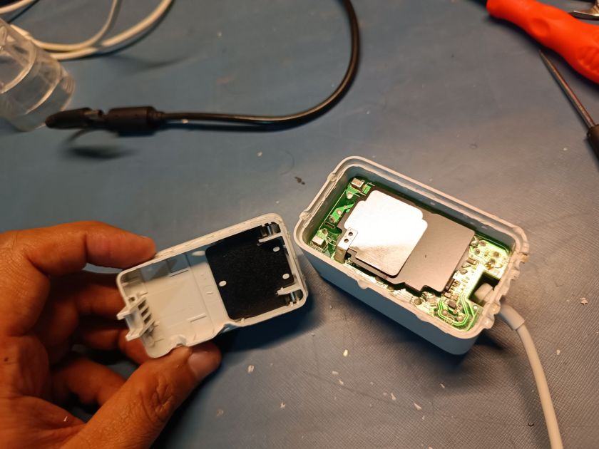
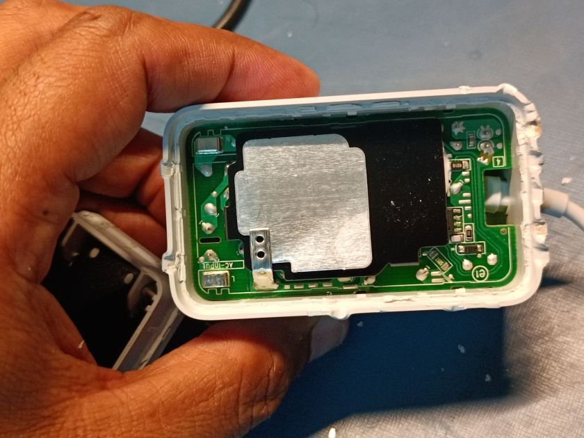
Bigger internal structure basically holds the main PCB from outside and inside it hold the speaker.

this aluminum plate is basically to spread the heat from the main processor board. You can see the thermal bad in the center.

Amazon Echo Dot 5th Gen Speaker Section


There is no mentioned about the ohms or wattage of the speaker anywhere just the QR code which has some internal part code I guess.


Amazon Echo Dot 5th Gen – Main Processor Board
The most interesting part in the device for many engineers is the main processor board. Everyone want to know which processor is used where they run their local AI engine, what is the RAM size, which and how much is the flash used, how did they do the Wi-Fi Connectivity, etc. So, let us dive in to that portion.
The processor board looks like this from the top. Here, what mostly you will see is a lor fo different power supply sections.
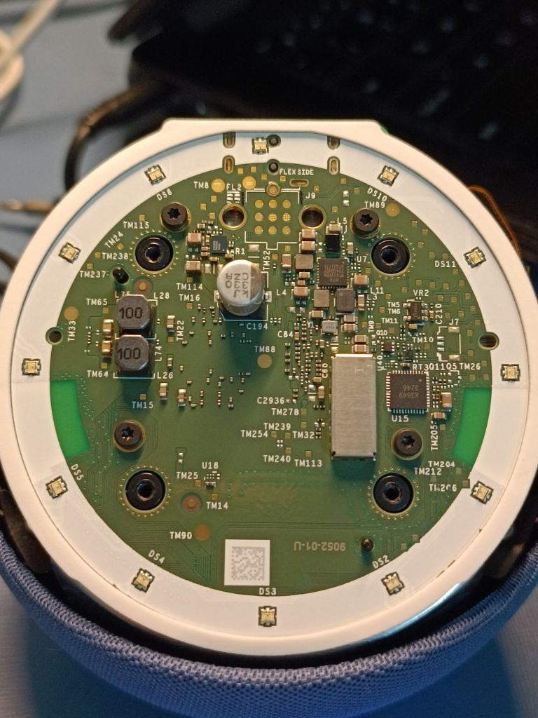
U7 is basically looking like a multiple rail dc dc converter IC from Mediatek Part number mentioned is MT6398BN, I could not find a datasheet on internet.

Another Shielded Power section(U10, L10) is there, shield is to reduce the emissions.


Besides this power supply you will find Audio Amplifier circuit which uses Analog Devices Maxim Integrated MAX98396EWB (U15). The Echo Dot speaker is driven by this Digital Input mono Class-DG Amplifier with an output power of 20W into 8 ohms / 19W into 4 ohms.

Another thing to note on this side of the PCB is the 12 RGB LEDs on the perimeter.
Now, let us see what is there on the bottom side of the Main PCB.
You can see J3 which is DC input jack, where you connect the power supply.
At the center is the main processor section which includes the processor(U1), DRAM(U3) and Flash(U4).
Amzon Echo Dot 5 uses an AZ2 processor, an updated version of the Amazon Neural Edge processor. It is marked MT8519BAAV, Micron NW942 Nand flash IC is used for the OS and data storage.
DRAM is provided with an SK Hynix H54926AY 0.5GB model with a 4266Mbps throughput.
and just below that you a PCB module, it is basically a Wi-Fi/Bluetooth module. You can see antenna on the PCB on both sides.

You can see the shield pads around this section, actually there was a shield, I just removed it.


Just below the processor section you have Wi-Fi connectivity module, in-house developed by the Amazon’s team.
It also uses a MediaTek Chipset (MT7653BSN).


There is Flex Cable which goes to the MIC array PCB I have shown you above.


And, that’s not all.
Amazon developed their charger also by themselves so I took it apart as well. Let me show you inside of the charger which is 15W charger (12V 1.25A), it has DC pin output connector.
Opening the enclosure was a tough game, you can see the battle marks 🙂


The black plate you see is nothing but a plastic separator, Aluminum sheet is for heat spreading.
The PCB is single sided as you will see in most of the power supply designs, to keep cost low. Looking at the PCB and components, design looks well designed, really good.
At the input AC side, you can see EMI filter is used and then using a bridge rectifier goes to the AC to DC power converter IC.
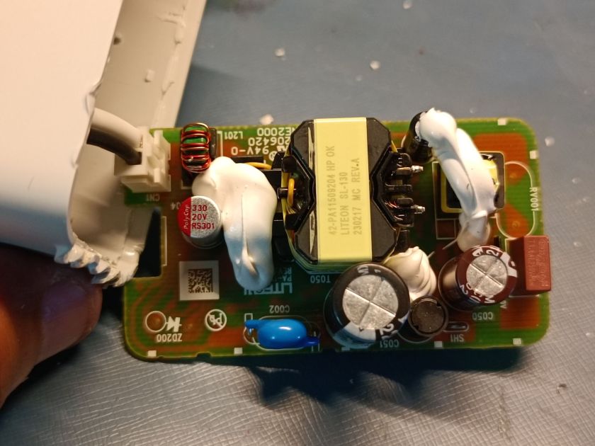
On the output side also you can see an inductor is used for post AC to DC filtering. this is not common to see in any low cost power supply or charger designs.
Quality of the transformer also looks really decent.


Bridge Rectifier RABS21

They have used Power Integration’s device (SC1616C) form its InnoSwitch Series.


Other than the InnoSwitch from Power integrations, there is another device used, you can see on the left side in the image below. IC Part number is SE120N10L2, looks like ideal diode.

That’s all from my side on this teardown. I hope you enjoyed reading and learned something new.
Do share with your friends so that they can learn too.
I am currently working as an embedded systems design consultant and helping companies build custom embedded products, develop test automation solution for their PCB.
If you have any feedback about the blog, you can share in the comments below or you can also contact me directly.
Excellent job, great info 🙏 Thank you for your time!!!
Thank you, Michael for your kind words and taking out time to read the blog.
Glad you found it interesting.
Does echo dot 5 work in Nigeria?
It should work. It only needs Wi-Fi to connect to the internet.
Good tear down. Lots of interesting information. So …were you able to assemble it all back again for it to work as before? 🙂
No, I did a deeper teardown with further hacking, so had to sacrifice 🙂
Very small size speaker high amount
You made me go deep inside the echo dot…good teardown