Previously, I did a detailed teardown on Boat Smart Watch and was amazed by the kind of engineering involved so I though of check some other designs like of MI Redmi Watch 2 Lite. It costed me 1799 INR from Amazon.
It is lower cost Smart watch with less features like it doesn’t have Bluetooth calling feature so MIC and speaker is missing. But, it has inbuilt GPS.
The Redmi Watch 2 Lite Smart Watch is a great budget-friendly smartwatch with a variety of features to help you stay active and healthy.

Let us see how the smart watch is constructed and the choice of components for various features.
What I don’t like about smart watch or fitness bad is it is not so easy to open them and most of the time it is destructive to open the device.
Redmi Watch 2 Lite Smart Watch Packaging
Packaging as good as any other consumer grade product. Product details are mentioned on the back side of the box or in the manual inside. Along with Smart Watch you get a USB magnetic charger cable as a standard accessory.


Smart Watch from outside
Before I start showing you inside, see how the smart watch looks from outside. Straps you need to remove by hard pressing buttons provided on the strap.


Once you open the Smart watch, as any other watch, it divides into two main parts the display and the main PCB/Sensor.
Smart Watch Display Panel with Capacitive Touch
Its a typical display with capacitive touch panel. Capacitive touch panel connects with display Panel via 6 pin FPC connector. It has I2C interface for Capacitive Touch. Touch IC part is removed but that nothing to worry. It’s a bought out item so nothing to design here.


I tried to open display and see how the display is from inside, I was expecting a backlight panel and glass display, what I found was multiple sheets.
One sheet I found which had large number of horizontal/vertical lines looks lines these are connecting traces for each pixel.

Smart Watch Display Panel Main Controller PCB
PCB has a large RF shield covering all electronics under that and RF shield is soldered, so it will be hard to remove :)Two wires you see are for the battery.


The PCB is attached to the enclosure with multiple small screws.
After removing screws, on the back side, what you get is a battery attached with double sided tape.

After de-soldering the battery wires from the PCB carefully I was able to see the part number and other details of the battery which are written on the other side.
BW20 is the Model, Its a Li-Ion Battery from Sunwoda Electronic Co Ltd, China. It’s rating is 3.87V and 262mAh 1.01Wathour Capacity

Back side of the main PCB has no components but some test pads and spring-loaded pins which connects to other parts like antennas, etc. See the image below.


I had to put a bit of an effort to open the shield on the main PCB. While doing that I also damaged some part of the board as well. See the images below


Now let us see what all components are there on the Main PCB.


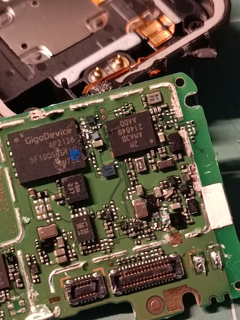

You can see in the image below. The main MCU is Apollo AMA3B from Ambiq Micro, which Apollo 3 Bluetooth MCU consumes only 6uA per Mhz.
Various inductors near AMA3B MCU is for dc dc converter inbuilt the MCU.


Board has a Gigadevices SPI NAND Flash 5F1GQ5R, 1Gbit Memory.
Two connectors one for display and other for the sensor.
On the board some more battery charger and buck-boost dc dc converter circuits are there.
I see 3 more ICs with part number difficult to identify but I am sure two are accelerometer and compass and one is probably SPI NOR Flash.

With GPS chipset part number I could not locate the datasheet. It is Synaptics SYN47752B1

See images below, it is interesting to see both GPS and Bluetooth antennas are Flex PCB antenna connected to main PCB via spring loaded pins


after removing the PCB, you get the base of the enclosure where further button, vibration motor, chargeing pins you will be able to see with connects to the main PCB.
At the center you see the sensor PCB with a flex cable with connector.


After removing the sensor PCB, you can see LEDs and PHOTO SENSOR with a front end IC which has a marking +AAAG. It will be a typical I2C SPO2 sensor front end.


One last thing, vibration motor was hidden inside the plastic enclosure and the connection is via Flex cable, spring loaded pins, connects to the main PCB.

A lot of other very small ICs are used on the main PCB which are basically load switchss for power management. Example: If you want to put off display, using load switch you can power off the display section, similarly other sections like Audio, sensor, etc.
So, that’s all in this teardown. I hope you enjoyed the details and got to learn something new today!
Subscribe to my blog, you will get an alert when I publish a new teardown blog.
I am currently working as an embedded systems design consultant and helping companies build custom embedded products, develop test automation solution for their PCB.
If you have any feedback about the blog, you can share in the comments below or you can also contact me directly.